


This is the EDA video you didn’t know you had been waiting for. I’m really keen to show this to our Zuken customers and the extended EDA community. Direct Gerber Import.
eCadstar offers users the ability to directly import Gerber data into the PCB environment. Why might you want to do this? Firstly, and this is its intended primary function; it gives you the opportunity to review your Gerber data without having to use an external viewer.
File new, pcb, pull in the gerber data. Review it. Maybe even panelise it and output again. Gerber in also gives you the opportunity to quickly import working gerbers from your PCB fabricator so you can very quickly review any manufacturing compensation that they might have applied ahead of OK’ing their master gerber’s for production. In addition to simply reviewing the data, eCADSTAR has a great feature set that allows us to very quickly and easily convert this flat unintelligent manufacturing Gerber data into valid, DRC compliant EDA data which we can use on our design. Perfect for reverse engineering a design from legacy Gerber data.
Basic Gerber import.
Layer by layer. First of all, I create a new PCB using an 8 layer stack up tech file. I’m also pointing to an existing schematic. I don’t really need either of those for a simple Gerber review. I don’t need the schematic and the PCB could be a simple single layer PCB but because we are going to review some enhanced functionality in the second part of this video I’ll use them now. First thing I do when I get into the new PCB, is to disable both DRC’s and change my routing grid to something very large. I’ll explain why the routing grid in a moment.
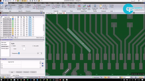
From the manufacturing Tab I can select: Photo Data Input. I’m going to import the Top, Primary side conductor layer first – Now the thing to note here is that for every single active layer in eCADSTAR you have an equivalent drawing layer. You don’t have to use these, you can define active layers for your drawing elements should you wish, but this is a good example of when to use an associated drawing layer. So I’m importing first Gerber file into my design. I’ll start with the top, primary side conductor. I’m importing this onto the conductor one layer in my PCB editor but remember it will be on the drawing elements of the conductor 1 layer. I’ve written a quick macro to bring the other 7 conductor layers in and as you can see I have customized my menu ribbon with some import features I use a lot and this import macro.
There that’s my 8 conductor gerbers imported. I chose to align them in a matrix, just for this demonstration but obviously, you can place them coincident to replicate your layout.

Now the second part which is really very neat. Let’s turn that flat almost unintelligent data into usable EDA data. There are just a couple of steps to do this. We are cautious in the electronics industry, and rightly so, about freely using the term ‘reverse engineering’ but most of us have been there at some point. Having to replicate a design from gerber data because the EDA tool it was created in, is obsolete or no longer available. Or the data has an unrepairable corruption or has even been lost.

But you still have the gerber data. That was sent out by the admin team who diligently archived it. Many many times I have been forced to use a silcon vendors layout otherwise they would not support us in production. The layout had to be identical to theirs. But they used a different EDA tool. We had access to gerber data but no way to directly import them. There begins an arduous conversion journey. Gerber to DXF. DXF in to EDA tool.
Can we convert the DXF data to intelligent EDA data within the tool? Usually not. So do we use the imported DXF data to essentially trace over? It’s all a compromise. Then just ahead of project completion you receive an update for this design and you need to repeat the process. It was a time consuming frustrating process. Or at least it was. eCadstars Gerber import will speed up any reverse engineering requirements you might have. Of course, you don’t even need a schematic and netlist. You can import the Gerber data. Convert it to the relevant conductor layers.
Position footprints directly from your library to align with the Gerber data. Note your library footprint pads do not need to be exactly the same as the pads on the imported Gerber data.
A trace in eCADSTAR makes its electrical connection as soon as it touches the pad. Not on the centroid of the pad. Once positioned use the Add netline command to add nets between pads. Utilising the 3D view you can then trace the connections back easily and continue adding the net connectivity at PCB level. You can even save and back annotate a node to node, pin to pin compliant schematic from this data. That’s Gerber import review and conversion in eCADSTAR. A very useful tool.