


 IPC CID Certified Interconnect Training
The mind boggles when you look around at the range of electronic equipment we use on a daily basis. This technology is not just relied upon but is often taken for granted and often abused as a result. Case in point – teenagers; recklessly discarding their smartphones and still assuming them to work.
I will, however, spare you the lecture but having had 27 years exposure to hardware development I fully understand the effort that has goes into the creation of that device; the hive mind collaboration during concept, the R&D effort during prototyping & development, the manufacturing expertise in production, right through to supply chain, distribution, compliance, qualifications and legal insight into market responsibilities usually all spread across a global team.
And then we consider the actual manufacturing process of components, PCB and final product assembly. All stages are particularly volatile and susceptible to environmental influences and marginal operational changes. A one or two centigrade variation in one process, can have a negative impact on production. An inaccuracy not seen during the production process could present itself only when the product is deployed in the field.
When an electronics outsider is introduced to modern PCB design & the assembly process it can be a hard concept for them to grasp. Many electronics graduates don’t have a full appreciation of the processes involved.
Without subjecting an industry outsider to too much tech talk I try to describe a single PCB trace: Take a piece of paper and draw 1cm. Most people have a good concept on visualising and replicating 1cm. Now take that and divide by 10 to give us our 1.0mm. That’s pretty small already. Now divide that 1.0mm into 10. Pretty small right? Impossible on paper to replicate, very hard to visualise. That is a typical width of a conductor trace on a regular consumer electronics product these days. Just 0.1mm. And they can be even smaller. There can be thousands of these all living next to each other, above and below each other delivering the sounds and images you want to see and hear on your phone.
But do you know how we take that trace from our EDA tool into production?
Well those traces are made using photography, drilling, plating, numerous, wet chemical processes with thermal cycles where the substrate material expands and contracts in each production phase. When the PCB is complete and the continuity of each of these tiny delicate copper traces is confirmed we then throw it at an assembly production line where temperatures regularly exceed 200 degrees C and we smother the whole thing in molten metal.
In essence, the process is a complex one, with strong potential for complications, which means the adherence of design rules become of paramount importance.
So how is this miracle of production actually achieved and what can we do to help ourselves?
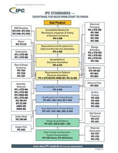 All of the people within the PCB layout, fabrication and assembly processes will have one thing in common. They will be striving to maximize production yield. To do this they will all adhere and work to the same international language: IPC standards.
Engineers will design footprints to IPC7351 standard, document their designs to IPC-2611/2 and IPC-2615, and export data in IPC2581. Whereas Fabricators select materials and processes based on IPC-4101, IPC-6012, J-STD-001, IPC-A-600. Where finally Assemblers and Testers will use IPC certified personnel and processes based on IPC standards.
So what is the benefit of all these standards and what do they mean:
- IPC-7351 standard provides guidelines for calculating pad dimensions
- IPC-2615: the definitive standard on printed board dimensions and tolerances
- IPC 4101 provides specification for Base Materials for Rigid and Multi-Layer Printed Circuit Boards
- IPC-6012 defines the Qualification and Performance Specification for Rigid Printed Boards
- IPC J–STD–001 highlights the requirements for Soldered Electrical and Electronic Assemblies
- IPC-A-600 provides guidelines for the Acceptability of Printed Boards
Learn and adopt the language and speak IPC!
How do I do that? Get qualified as an IPC CID (Certified Interconnect Designer) or IPC CID+ (Certified Interconnect Designer – Advanced) engineer.
For more information please contact us today!