


To maximise the performance of a circuit design, the implementation of track length matching is key. In any circuit design, an electronic signal takes a certain amount of time to travel along the conductor to reach its end destination. It is crucial to identify the sections of a printed circuit board (PCB) design that requires length matching to guarantee that the signals arrive with accurate timing.
Track length matching is normally thought of as in pairs, but it also applies to buses with single-ended signals and differentially-driven buses. As CPU peripherals and other digital systems require faster-operating speeds, the propagation delays in a high-speed system, places tight tolerances on the allowed track length in a conductor carrying digital signals.
This article explores Quadra’s best practices for applying track length matching.
So, what is Track length matching?
As the name suggests this is the laying out of a design that matches the lengths of two or more PCB tracks, also known as traces. These groups could be one of the following:
- Single-ended tracks routed in parallel.
- Differential pairs.
- Multiple differential pairs in parallel.
- Clock signals in either single-ended or differential pairs in parallel.
PCB tracks carrying digital signals do not necessarily need to be perfectly length matched. With copper surface layer tracking there will always be an amount of jitter on the rising edge, preventing signals routed in parallel to be perfectly length matched. The end goal is to reduce the length or timing mismatch below limiting values. The allowed length mismatch and timing mismatch are related to the signal velocity.
Is your PCB Design Software helping or hindering you?
Speak to Quadra about eCADSTAR and how it is helping customers around the world to create better and more effective PCB designs
Talk to our team 01254 3018888
How do you know what track length is optimum?
Component datasheets, signalling standards and interface standards are key. There is so much standardisation these days that most high-speed components use one of the many signalling standards. Manufacturers should always have impedance and routing specifications available.
A length mismatch can also be converted to a timing mismatch using signal velocity, although extreme care must be exercised when selecting the velocity of a digital signal. Modern digital signals, generally run with edge rates much less than 1 ns, will have bandwidths reaching into the high GHz, and will only tolerate very small mismatches. Dispersion in the PCB substrate causes the signal velocity to vary with frequency. For example, FR4 exhibits normal dispersion below ~1 GHz, so lower frequencies will arrive at the receiver earlier than higher frequencies.
Clock Signals
Using system clocks to trigger every device in a chain of components is extremely difficult in large designs. This is, in part, due to the fact that each integrated circuit has different logic gate delays and rise timing. Typically, modern digital components use source synchronisation or embedded clocks. For embedded clocks signals it is best practice to route a track alongside the parallel data track. The clock tracks also need to be length matched to other data tracks.
Track length matching to prevent skew on parallel data buses
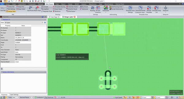
Skew simply refers to a timing mismatch between the rising edges of two or more digital signals in a parallel bus. The signal propagating on the shortest trace will arrive earliest, triggering a downstream gate before the other signals on the bus. eCADSTAR allows you to define buses and differential pairs at the schematic stage, enabling you to enforce track length matching your layout which will keep any skew within tolerable limits.
Length matching in multiple single-ended nets is straightforward. Adding tuning structures to all tracks on the bus ensures they are the same end length.
If you have multiple differential pairs carrying parallel data, each differential pair must be matched, and the pairs then need to be matched to each other.
What About Analogue Differential Signals?
Analogue signals can also be routed as differential pairs; however, it is less common even at very high frequencies. Some manufacturers offer differential op-amps for high GHz bandwidth allowing for easier routing of analogue signals around a board.
Analogue differential signals require accurate length matching, just like digital differential signals. The difference is that analogue differential signals resemble 3-phase AC wiring, where an adjacent analogue ground plane is used as a reference for both ends of the pair. While digital signals do not explicitly need a ground plane, placing a ground plane adjacent to the digital differential pair is beneficial for the reasons outlined above.
eCADSTAR – Built to Help You Deliver Results
- PCB DE64-bit computing
- Mouse and touch screen operation
- Powerful graphics, enabling users to design in a native 3D environment
- Advanced Collaborative design, allowing design activities to occur concurrently
- 2D and 3D environments
- Multi-core processor